Scanning Electron Microscope (SEM)
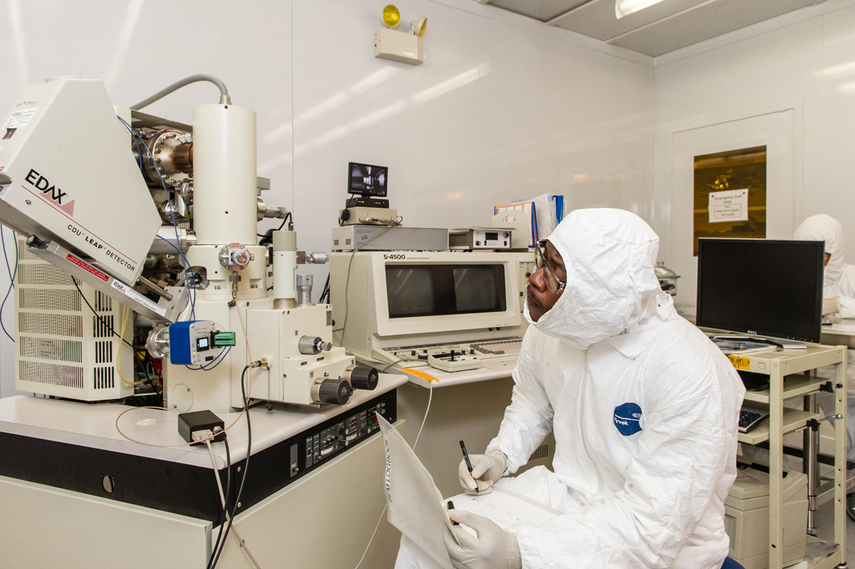
Hitachi S-4500 II Cold Field Emission Scanning Electron Microscope
This FE SEM is used to image features at magnification ranging from 20x to 500,000x.
Resolution depends on operating conditions:
- 1.5 nm (at 15 kV accelerating voltage, WD 4 mm)
- 4.0 nm (at 1kv accelerating voltage, WD 3mm).
Accelerating voltage can vary continuously from 0.5 kV for resist imaging to 30 kV for EDS detection and metallic surface imaging.
Stage motion ranges:
- X: 0 to 100 mm
- Y: 0 to 50 mm
- Z: 3 to 28 mm (continuous)
- Tilt: -5º to +45º
- Rotation: 360º (continuous)
The image capture software was updated in 2003 with Quartz PCI version 5.1.
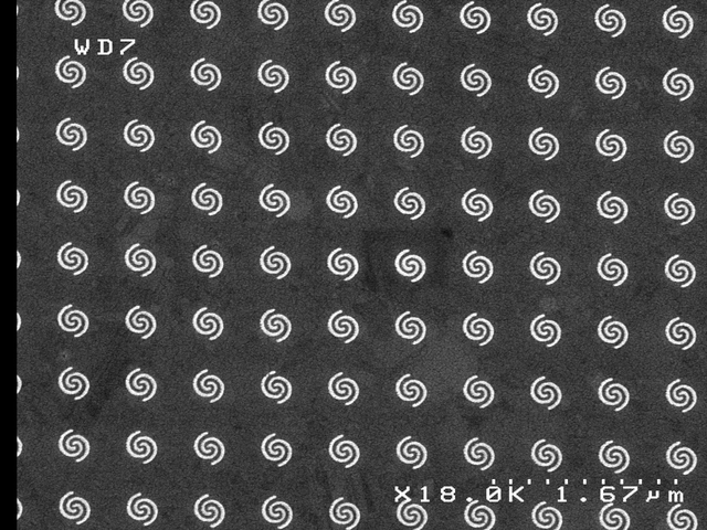
Image: Al nano spirals fabricated by Tiago Ramos Leite da Silva , ChE LSU
PDF documents:
- SEM Procedures.pdf (SEM Standard Operation Procedures)
- The Compact Detector Unit.pdf (EDAX detector information)
For more information, questions or training please contact Sergi Lendinez